
COMMON SOLDERING ISSUES
Following are common soldering issues that may occur during solder training or production operations.
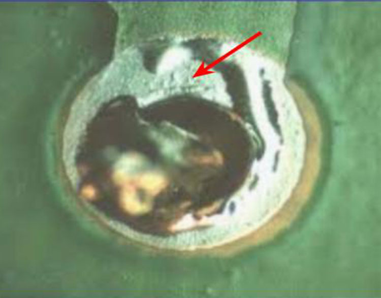
Pad Contamination (1)
Cause: Inadequate removal/cleaning of flux residue after reflow.
EPEC
Correction: RMA flux residues must be removed from the
assembly. On some assemblies or locations, no-clean fluxes
must also be removed.
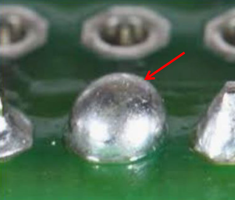
Excess Solder (2)
Cause: Excess solder was applied to the connection during soldering.
adafruit.com
Correction: Remove excess solder using fluxed
solder wick and soldering iron or a solder sucker.
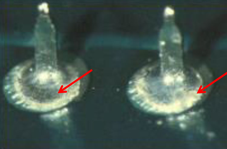
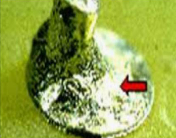
Insufficient Wetting (3)
Cause: Insufficient heating of the original solder connection.
NASA
Correction: Flux the connection on both side of
the PCB. Connect both the pin and pad with a
soldering iron and reflow. Add solder as
necessary.
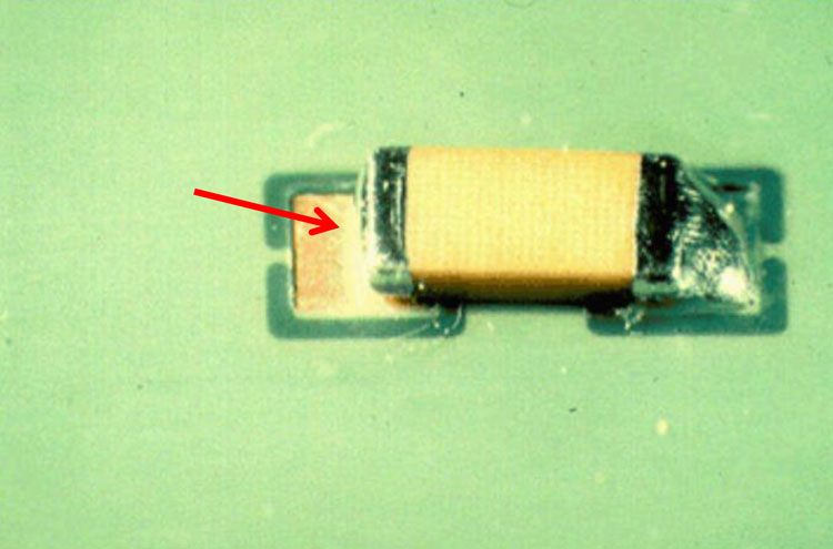
Poor Wetting (4)
Cause: Surface contamination on the soldered surface.
visioneng.com
Correction: Clean both sides of the PCB with PCB
cleaner and brush. Flux both sides and reflow from the
bottom side. Add solder as required.
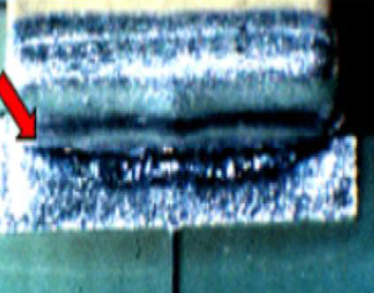
Solder Tear (5)
Cause: During solder solidification, solder may separate at the grain
boundary as it contracts. More common in lead free solders.
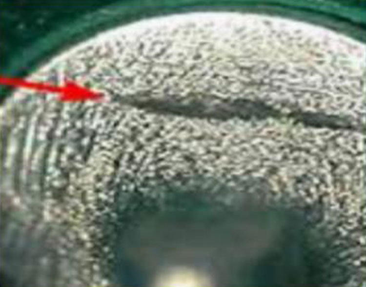
NASA
Correction: IPC-610H states there is no defect
associated with this anomaly provided the
connection meets all other acceptance criteria.
Poor Wetting (6)
Cause: Poor solder wetting/contamination
on the component/land terminations.
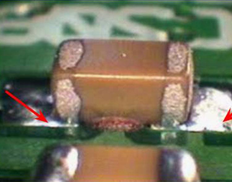
visioneng.com
Clean the component and both ends with
PCB cleaner and brush. For resistors, flux and reflow
each end. Add solder as necessary. For chip caps, use
hot air reflow.
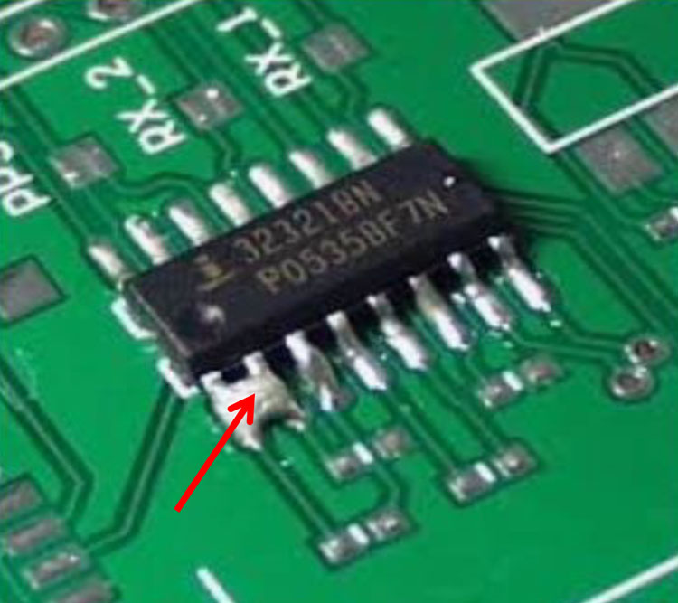
Solder Bridge (Short) (7)
Cause: Excessive solder between adjacent leads.
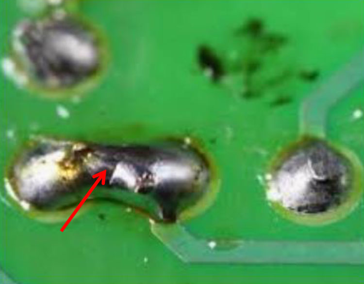
Pimoroni, Youtube-Androkavo
Correction: Flux both connections. Contact soldering iron tip onto
both leads to reflow solder and eliminate solder bridge. Clean both
leads of residual flux.
Chip Component Side Overhand "A" (8)
Cause: Incorrect side placement of the chip component
on it's mounting pads.
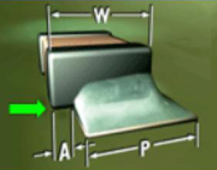
NASA
Correction: IPC-610H specifies Maximum Side Overhang
of 50%(W) for Classes 1 and 2.
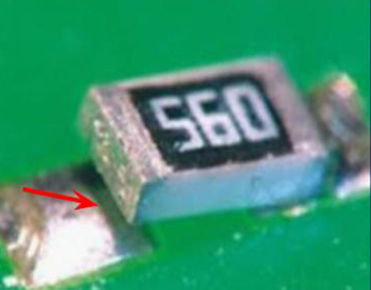
Insufficient Solder (9)
Cause: Insufficient solder application during hand soldering.
autodesk.com
Correction: IPC-J-STD-001H specifies minimum solder filler height
on 1, 2, 3 and 5-sided chip components for
Class 1 and 2 applications.
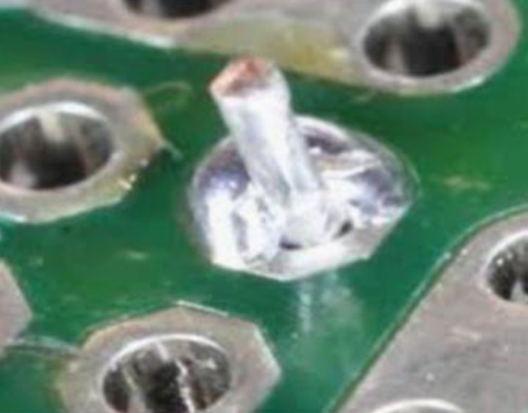
BGA Cold Solder Joints/Open Joints (10)
Cause: Insufficient heating of the BGA solder balls during BGA reflow (melting).
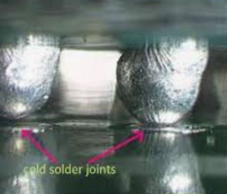
emerald.com
Correction: BGA Cold Solder and Open connections
are not repairable. BGA must be removed and
replaced with new or re-balled BGA.
Solder Short (11)
Cause: Application of excess solder during hand soldering.
autodesk.com
Correction: Flux the connection and use a soldering iron to
draw off excess solder. Or, remove the excess solder
using solder wick and soldering iron.
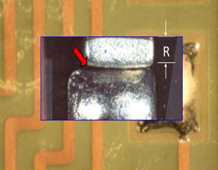
Insufficient Fillet Height (12)
Cause: Insuffiecient solder applied to chip
component end joint termination.
NASA
Correction: For Classes 1 and 2, J-001H requires that solder
be evident on the vertical surface of the termination.
Cold Solder - Solder Paste (13)
Cause: Incomplete reflow (melting) of solder
paste balls during the reflow cycle.
NASA
Correction: Flux the lead, pad, and topside. Reflow lead
and pad by concurrent contact with the soldering iron.
Insufficient Wetting (14)
Cause: Solder has not wetted the pin and
partially wetted the pad.
adafruit.com
Correction: Flux the lead/pad. Verify even heating and
reflow of the lead and pad by concurrent contact with
the soldering iron. Clean both sides.
Tombstoned Component (15)
Cause: Imbalance of solder joint surface tension in molten
solder causes the "stronger" joint (right side) to lift the
component off the board, creating the "tombstone".
cadence.com
Correction: Correct this defect by fluxing and reflowing the chip
component using hot air or thermal tweezers (not on chip caps).
Or, alternate reflow of fluxed chip terminations via soldering iron.
Chip Component End Overlap (16)
Cause: Misplacement of the chip component end
placement on its mounting pads.
EPEC
Correction: J-001H requires "Minimum End Overlap" for
classes 1 and 2.
CONTACT AEIC
AEIC provides IPC CIS certifications to wide range of clients. These include military contractors, consumer electronic suppliers, OEM & EMS suppliers, and individuals seeking personal certifications.